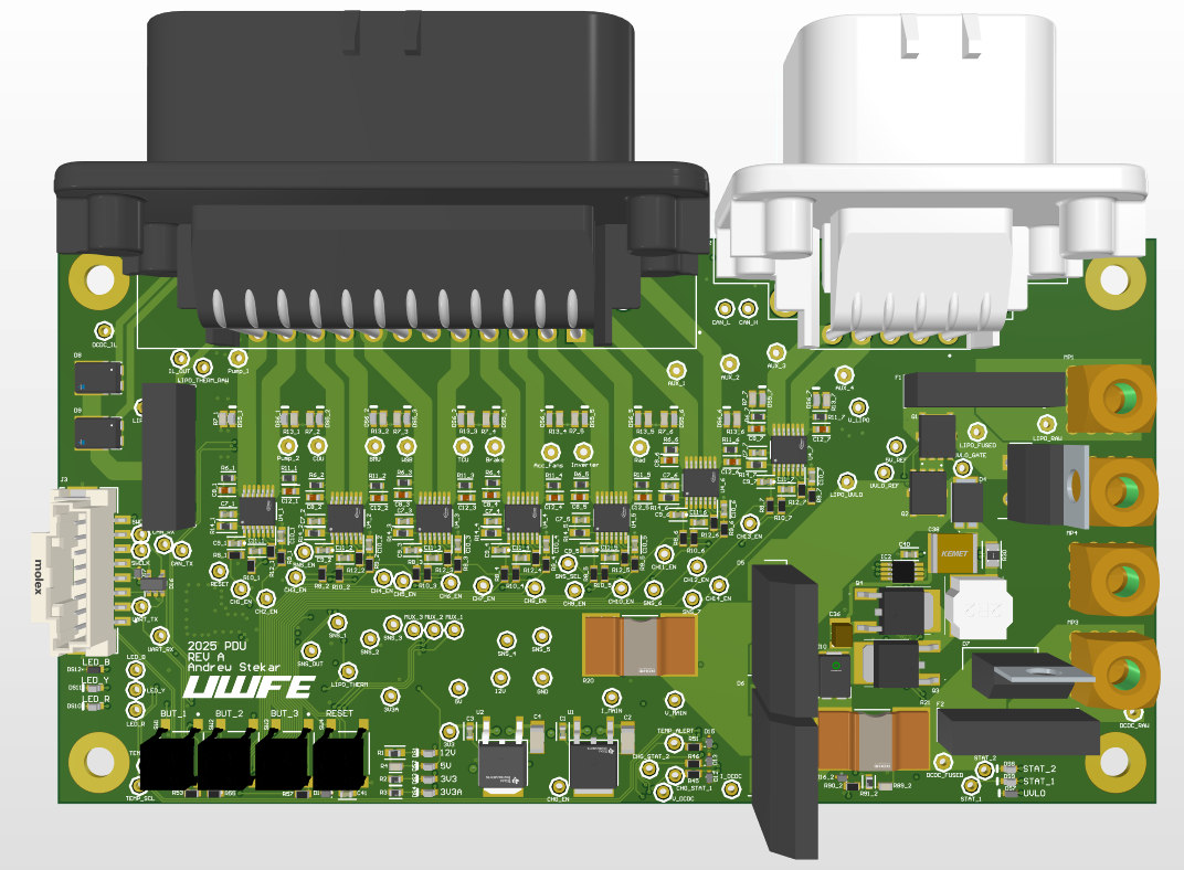
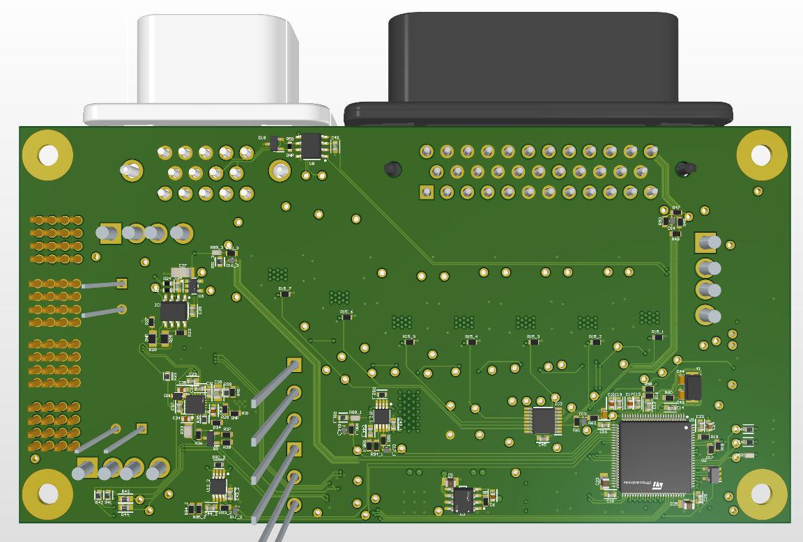
Project Details
- Redesigned our low-voltage power distribution PCB. The board has the follwing features:
- can supply up to 40A continuously to 14 separate loads (7.5A max per load)
- load switching capabilities to seamlessly switch between our DCDC and backup battery sources
- a charging circuit that charges our battery while the DCDC is supplying power
- E-fused load channels, which will attempt to reset themselves before fully faulting the car in case of a glitch (previously used blade fuses).
To enhance performance, I chose to use a 6-layer stack-up and to isolate the analog and high-speed digital signals on opposite sides of the board. I did my best to minimize the loop size of these sensitive traces as this will reduce noise from coupling, increasing current sense accuracy. I also prioritized adding a significant number of test points to assist in debugging and bring-up of the board.